For industry alerts, click here.
4th CMC Seminar Focus on Materials Quality
Quality Excursions Can Cost Fabs Hundreds of Millions of Dollars
San Diego, CA, Aug 15, 2019: The Critical Materials Council (CMC), a unit of TECHCET, announces that their 4th annual public CMC Seminar will be focused on quality excursions and the global materials value-chain. Fabs such as local Taiwanese powerhouse TSMC have suffered millions of dollars in lost product revenues due to quality excursions in materials from global materials suppliers. The CMC Seminar is one of the best forums to learn about these challenges and opportunities related to evolving electronic materials supply-chains.
The CMC Seminar explores the dynamics of local materials supply-chains within global markets. Along with a panel discussion between invited CMC fabs and material suppliers and networking opportunities, there will be timely presentations on the following topics:
• Keynote on “Navigating Global and Local Semiconductor Materials Markets and Supply-Chains,” presented by Mr. KC Hsu, Vice President of Micron Memory Taiwan,
• “Bulk Specialty Gas Supply: Debottlenecking the Electronics Material Supply Chain From Material Production to Fab Consumption,” by Dr. Hok Tsan Lam, Head of Business Development for
Linde Electronics,
• “Solving Challenges in Vapor Concentration Delivery,” by Mr. Ray Morgan, Director of Veeco,
• “Prevention & Control of Particles & Heavy Metal Contamination in Fabs,” by Dr. David Huang, Vice President of Pall Filters,
• “Global Materials Markets and Forecasts,” by Dr. Dan Tracy, Sr. Analyst of TECHCET, and
• “Challenges of Global Supply Chains,” by Ms. Jenny Tan, Sr. Manager for Global Procurement of Micron.
Attendees will have opportunities to network with CMC Fab members who will have just finished their private face-to-face meetings held earlier that week.
Who Should Attend?
• I. Semiconductor device fabricators,
• II. Materials and equipment suppliers, and
• III. Financial analysts, with an interest in semiconductor process materials markets.
For more information and to register for the event: CMC Seminar 2019
CMC Fab members include:

Micron VP Keynote for the 4th CMC Seminar
Event in Taiwan 17 October will feature a keynote from Micron Technologies
San Diego, CA, August 13, 2019: The Critical Materials Council (CMC) of semiconductor fabricators is pleased to announce that the keynote presentation for the 2019 CMC Seminar will be “Navigating Global and Local Semiconductor Materials Markets and Supply-Chains,” presented by Mr. KC Hsu, Vice President of Micron Memory Taiwan. The public CMC Seminar will be held on October 17th at the Fullon Hotel A8 in Taoyuan, Taiwan. Attendees have the opportunity to network with CMC Fab members who will have just finished their private face-to-face meetings held earlier that week.
The CMC Seminar focuses on the dynamics of local materials supply-chains within global markets. Global fabs and suppliers are increasingly challenged in managing materials requirements, quality control, and logistics issues across many regions. The CMC Seminar is one of the best forums to get information on the rapidly growing electronic materials supply-chain within Greater China and Asia at large.
Who Should Attend?
I. Semiconductor device fabricators,
II. Materials and equipment suppliers, and
III. Financial analysts, with an interest in semiconductor process materials markets.
For more information and to register for the event: Please Click here
US$1B Global Market for Quartz Growing Amidst Fluctuating Lead-times
Wafer Shortage affecting Silicon Components Market
San Diego, CA, July 25, 2018: TECHCET—the advisory services firm providing electronic materials information— announced that the global market for consumable quartz components used in semiconductor manufacturing equipment in 2017 was over US$1 billion in revenues, having grown 26 percent from 2016. Some lead-times for delivery in 2017 doubled due to the high demand, and the supply-chain is still constrained for hot-work parts. The market for fabricated quartz parts in 2018 will continue to be strong, although growing at a lower rate of 9 percent over 2017, and with longer-term CAGRs moderating. The consumable silicon components market, at about half the size of the quartz market, shows similar dynamics. Recent silicon material price spikes are expected to normalize as we move into 2019, detailed in the latest TECHCET Critical Materials Reports (CMR) for quartz and for silicon equipment components.
“The silicon materials market now has a healthy number of suppliers that compete for fabs shopping for spare parts. However, some suppliers will likely not be able to survive the next correction, if the supply-chain keeps growing. The recent raw material price increases due to the silicon wafer shortage have been difficult for the supply-chain to absorb,” explained Kuang-Han Ke, TECHCET senior analyst and author of the report. “Meanwhile, quartz supply and demand seems to have returned to a healthy balance, and the leading suppliers are working hard to differentiate their portfolios with new base material offerings.”
Quartz parts suppliers covered in this report include: Applied Ceramics, Beijing Kaide Quartz, DS Techno, Ferrotec, GM Associates, Han Yung, Hangzhou Dahe Thermo-magnetics, Hayward Quartz Technology, Heraeus Quarzglas, Heraeus-Shin-Etsu Quartz Products (HSQP), Hsin Yui Technology, Kumkang Quartz, Maruwa, Quality Quartz Engineering, Quick Gem Optoelectronic S & T (QGOE), Shin-Etsu Quartz, Techno Quartz, TOSOH Quartz, Worldex Industry & Trading (West Coast Quartz), WONIK QnC, and Xycarb Ceramics.
Silicon parts suppliers covered in this report include: Applied Ceramics, Atecom Technology, CoorsTek, DS Techno, Ferrotec, Global Wafers (SunEdison Semiconductor), Hana Materials, Hayward Quartz Technology, IMS Daewon, SKC Solmics, Sanwa Engineering, Silfex, Siliciumbearbeitung Andrea Holm, SungRim, Techno Quartz, Thinkon Semiconductor, Worldex Industry & Trading (West Coast Quartz), Xycarb Ceramics, and Yerico Manufacturing.
Purchase Reports Here: https://techcet.com/product-category/consumable-equipment-components/.
2018 CMC Seminar / ICMtia Conference Joint Event in Ningbo, China
SAVE THE DATE: October 30-31, 2018
San Diego, CA, July 09, 2018: TECHCET—the advisory services firm providing electronic materials information— announced that the 2018 Critical Materials Council (CMC) Seminar will be held in Ningbo, China in coordination with the IC Materials and Components Industry Technological Innovation Alliance (ICMtia) of China’s annual event. This will be a joint conference 2-day event, October 30-31, for registered attendees and members from both the ICMtia and CMC. Following this public event will be 1.5-days of private CMC face-to-face meetings.
“We are very happy to be working with the ICMtia, who will be hosting the event in Ningbo, China, for the mutual benefit of both our member organizations,” said Lita Shon-Roy, TECHCET President and CEO. “IC fabrication is a global business based on global supply-chains, and our events will cover pre-competitive best-practices in ensuring quality, safety, and trace-ability in semiconductor fabrication materials.”
“We are excited that the CMC Seminar and private meeting will be located in Ningbo this year, and look forward to meeting the CMC Members,” commented Ingrid Shi, ICMtia Secretary General. “SMIC, China’s largest IC wafer foundry company, has committed to promoting the development of the IC industry supply-chain in Ningbo, less than 200 kilometers south of Shanghai on the coast.”
The first phase of construction to support IC manufacturing, including materials, parts, and other special projects is planned to be completed and put into use in 2018. Located in the Beilun Chaiqiao District of Ningbo, regions are divided into high-end manufacturing and production areas, R&D service complexes, and ecological and cultural areas. When including the Lingang Chemical District and the development of space on the south side of the region, the planned area can reach 35 square kilometers.
Event information: https://cmcfabs.org/cmc-events/
ABOUT TECHCET: TECHCET CA LLC is an advisory service firm focused on process materials supply-chains, electronic materials technology, and materials market analysis for the semiconductor, display, solar/PV, and LED industries. Since 2000, the company has been responsible for producing the SEMATECH Critical Material Reports, covering silicon wafers, semiconductor gases, wet chemicals, CMP consumables, Photoresists, and ALD/CVD Precursors. For additional information about these reports or CMC Fabs membership please contact Diane Scott at info@cmcfabs.org +1-480-332-8336, or go to www.techcet.com or www.cmcfabs.org.
ABOUT ICMtia: IC Materials and components industry Technology Innovative Alliance (ICMtia) is a Chinese organization promoting the production, application, research and development of IC materials and components in industry. The alliance is also trying to build up the domestic material and components supply chain and stimulating cooperative development. The organization is a non-exclusive, non-profit that guarantees fairness, impartiality, and sustainable development. The alliance was established in 2012. For additional information about ICMtia activities please contact Manyu Dai at manyu_dai@icmtia.com +86-574-86120213 or go to www.icmtia.com.
ALD/CVD Precursors Market Reaches $1.3B by 2023
Cobalt sources highly strategic through 2023
San Diego, CA, July 3, 2018: TECHCET—the advisory services firm providing electronic materials information— announced that strong growth in IC fabrication demand for atomic-layer deposition (ALD), chemical-vapor deposition (CVD), and spin-on dielectric (SOD) precursors should result in a combined global market size of US$1.3 billion by the year 2023. Specifically, metal precursors are expected to see a compound annual growth rate (CAGR) of 6.2 percent through 2023 starting from $460 million in revenues for this year, as detailed in the latest TECHCET Critical Materials Report (CMR). The market for dielectric materials is forecasted to be $465 million this year with CAGR of 8.2 percent through 2023, as detailed in the latest CMR.
“Plasma enhanced CVD and ALD processes drive increasing demand for silicon precursors, used in depositing the 32-72 layers of 3D-NAND chips and in self-aligned multiple patterning for advanced logic and memory chips,” explained Dr. Jonas Sundqvist, TECHCET senior analyst and author of the report. “We see a need for more advanced ALD/CVD precursor production in China, to support more leading-edge logic and memory fabs ramping production there.”
Cobalt (Co) metal is being used to encapsulate copper on-chip multi-level interconnects in the most advanced logic fabs for both foundries and IDMs. Intel is using full cobalt interconnects to replace some of the copper levels in it’s newest logic chips. The conservative demand forecast for cobalt metal in the form of ALD/CVD precursors for logic IC fabs is $25 million in 2018, with considerable growth to $70 million by 2023.
Due to the competitive demand for cobalt needed for the lithium batteries used in EVs, and due to conflict issues in the supply-chain, cobalt metal pricing is volatile and reliable forecasting is correspondingly difficult. To anticipate supply:demand imbalances, TECHCET tracks ALD and CVD precursor demands in competing high volume manufacturing (HVM) industries such as flat-panel display, photovoltaics, MEMS, and LED.
Suppliers covered in this report include: Adeka, Air Liquide, Azmax part of Azuma group, BASF, DNF “Dream New Future”, Dow Corning, Digital Specialty Chemicals (DSC), DowDuPont, Entegris, Epivalence, FujiFilm, Gelest, H.C. Starck, Kojundo Chemical Laboratory, Merck’s EMD Performance Materials, Nanmat Technology, Norquay Technology, Nova-Kem, Nanogen Solutions, Pegasus Chemicals, Praxair, Soulbrain, STREM, TCI Chemicals, Tri Chemical Laboratories, Umicore, UP Chemical, Versum Materials.
Purchase Reports Here: https://techcet.com/product-category/ald-cvd-precursors
Freeman and Tracy Enrich Ranks of TECHCET Analysts
Far-sighted Experts Recently with Gartner and SEMI, respectively
TECHCET—the advisory services firm providing electronic materials information— announced that seasoned industry experts Dean Freeman and Dan Tracy have recently joined the firm as senior analysts. Freeman was most recently a Market Research Vice President for Gartner, and now covers Silicon Wafer markets and related supply-chains for TECHCET. Tracy was most recently the Senior Director of Industry Research and Statistics for SEMI, and now covers Sputter Targets markets and supply-chains for TECHCET.
“TECHCET maintains a laser-like focus on anticipating and mitigating critical materials issues for the benefit of the Critical Materials Council (CMC) and the global industry at large,” said TECHCET President and CEO Lita Shon-Roy. “Adding Dean and Dan to our team of semiconductor materials analysts allows us to increase our coverage of the critical issues associated with maintaining existing supply-chains, as well as integrating new materials into global IC fabs.”
Dean W. Freeman has over 30 years of semiconductor manufacturing and materials expertise, including work in a fab and for semiconductor equipment manufacturers. He had responsibility for every aspect of the semiconductor manufacturing process, from wafer selection to final passivation. Prior to Gartner, he worked at FSI, Watkins Johnson, Lam Research, and Texas Instruments. Freeman has nine patents, a B.S. in Chemistry and Earth Science from Whitworth College, and a M.S. in Physical Chemistry from University of Nevada Reno.
Dr. Dan P. Tracy has over 30 years of materials engineering and market research experience in semiconductor manufacturing. In his role with SEMI, he hired and managed a global market research team of four that provided globally recognized market intelligence and services to member companies and others. Prior to his 18 years with SEMI, he learned the dynamics of IC fab markets by working with Dan Rose of Rose Associates on materials forecasts. Tracy has a B.S. in Chemistry from State University of New York, an M.S. in Materials Science and Engineering from Rochester Institute of Technology, and a Ph.D. in Materials Engineering from Rensselaer Polytechnic Institute.
Over $40B Fab Materials Market Led by Silicon Wafers
Silicon wafer revenues grew 21% in 2017
San Diego, CA, June 08, 2018: TECHCET—the advisory services firm providing electronic materials information— announced that global semiconductor wafer fabrication process materials market grew by 9 percent year-over-year (Y/Y) to reach US$41.4 billion in 2017. Silicon wafers are one of the main drivers for this growth, with the cumulative area of all wafer sizes shipped in millions of square inches (MSI) growing 9.9 percent Y/Y, along with revenues increasing 21 percent. The forecasted growth for 2018 of MSI and revenues are estimated at 6 percent and 22 percent, respectively, as detailed in the latest TECHCET Critical Materials Report (CMR) on Silicon Wafers.
Silicon wafer supplier activities include the following:
o GlobalWafers is operating at full capacity, which will increase by 7 percent in 2018,
o Siltronic and SUMCO are both increasing capacity, and
o New Chinese entrants to the market will add over 1.2 million WSPM by 2020 potentially creating a significant oversupply in the market.
“Global semiconductor wafer revenues increased by 36 percent year-over-year in the first quarter of 2018, so the industry should be able to fund additional capacity,” commented Dean Freeman, TECHCET senior analyst and author of the report. “SEH is the only Top-6 supplier to have not yet made an expansion announcement, however it is very likely that they will add capacity to defend their top market-share position.”
TECHCET’s proprietary wafer-demand forecast predicts a deficit in supply through the year 2020 and possibly into 2021. Semiconductor fabs producing devices on 150mm and 200mm diameter wafers are now running at maximum capacity, and are expected to maintain high demand for silicon. Wafers <=150mm in diameter saw MSI growth of 19 percent Y/Y, while 200mm wafers experienced healthy growth of 15 percent Y/Y. Suppliers covered in this report include: Ferrotec, GlobalWafers/SunEdison, Hemlock Semiconductor (HSC), National Silicon Industry Group (NSIG) of China, Okmetic Ojy, Shin Etsu Hondotai (SEH), Siltronic, SK Siltron, SUMCO, Wacker Chemie AG, and Wafer Works. Purchase Reports Here: https://techcet.com/product/silicon-wafers/
CMP Materials Market to Reach $2.4B by 2022
Slurry and Pad Sub-Markets both ~6% CAGR
San Diego, CA, January 18, 2018: TECHCET—the advisory services firm providing electronic materials information— announced that increased use of 3D structures in commercial ICs leads to the need for more Chemical-Mechanical Planarization (CMP) process steps in commercial IC fabrication to keep the different layers properly aligned. The growing importance of CMP technology will lead to steady growth in the market for consumable materials. In particular, colloidal ceria slurry technology is a growing opportunity for 3D-NAND fabrication, as detailed in the latest quarterly update to the TECHCET Critical Materials Report (CMR) on CMP Slurry and Pads.
“The number of CMP process steps from 28nm- to 10nm-nodes has doubled, and advanced nodes clearly offer more opportunities for CMP and the need for more process consumable products,” explained Diane Scott, TECHCET senior analyst and author of the report. “Based on our proprietary models, at and below the 14nm-node the transistor-level CMP steps exceed the number used to form metal interconnects.”
Due to the recent introduction of cobalt (Co) metal for on-chip interconnects, TECHCET is now tracking direct materials for Co CMP. The rapidly growing market for cobalt CMP slurry is estimated to be about US$4M this year, using slurry sets derived from those used in copper (Cu) CMP. Global slurry and pad revenues for all IC CMP processes are forecast to reach US$2.4 billion by the year 2022.
Suppliers covered in this report include: Ace Nanochem, Adcon Lab, Anii Microelectronics, Asahi Glass, BASF, Bailkowski/PSB, Cabot, Dongjin SemiChem, DowDupont, Eka Chemical/Akzo Nobel, Eikem, Eminess Technologies, Entrepix, Evonik Industries, Ferro, FujiFilm, Fujimi, Fuso Chemical, General Engineering and Research, W.R.Grace, Hitachi Chemical, Innovative Organics, Intersurface Dynamics, JGC C&C, JSR, KC Tech, Kemesys, Merck (incl. former AZ Chemical), Mitsui Mining & Smelting, Nalco, Nano Phase Technologies, Nissan Chemical Industries, Nitta-Haas, Precision Colloids, Rhodia (Solvay), Samsung (Cheil Industries), Showa Denko, Sibond, Saint-Gobain, Soulbrain, UK Abrasives, U Wiz Technology, Universal Photonics, Versum, Wacker Chemie
Purchase Reports Here: https://techcet.com/product/cmp-slurry-and-pads-only/
ABOUT TECHCET: TECHCET CA LLC is an advisory service firm focused on process materials supply-chains, electronic materials technology, and materials market analysis for the semiconductor, display, solar/PV, and LED industries. Since 2000, the company has been responsible for producing the SEMATECH Critical Material Reports, covering silicon wafers, semiconductor gases, wet chemicals, CMP consumables, Photoresists, and ALD/CVD Precursors. For additional information about these reports or CMC Fabs membership please contact Diane Scott at info@cmcfabs.org +1-480-332-8336, or go to www.techcet.com or www.cmcfabs.org.
CMC Conference 2018 Call For Papers
Semiconductor manufacturing event to be held April 26–27 in Phoenix, Arizona
San Diego, CA: The Critical Materials Council (CMC) of semiconductor fabricators and TECHCET announce a Call For Papers (CFP) to be presented at the 2018 CMC Conference, April 26-27, 2018 in Phoenix, Arizona. Like the first two CMC Conferences held in Dallas and Portland (cmcfabs.org/cmc-events/), the 2018 event will cover actionable technical and supply-chain information related to critical materials for global semiconductor fabs.
KEYNOTE: David Bloss, Vice President, Technology and Manufacturing Group Director, Lithography Technology Sourcing, Global Supply Management, Intel Corp.
Three sessions will cover the following themes:
- Global supply-chain issues of economics and regulations,
- Immediate challenges of materials & manufacturing, and
- Emerging materials in R&D and pilot fabrication.
Attendees will include industry experts handling supply-chains, business-development, R&D, and product management, as well as academics and analysts. CMC member companies (http://cmcfabs.org/members/) will be attending this meeting, as it is an important part of their membership.
To submit a paper for consideration, please send a 1-page abstract by January 15, 2018 to cmcinfo@techcet.com.
On behalf of the CMC Conference committee,
Lita Shon-Roy, Jonas Sundqvist, Ph.D., Ed Korczynski
For more information on CMCFabs or CMC Associate Memberships, please contact Mike Walden at cmcinfo@techcet.com. For information on sponsoring the CMC Conference please contact us at cmcconf@techcet.com, +1-480-382-8336 x1.
ABOUT TECHCET AND CRITICAL MATERIALS COUNCIL: TECHCET CA LLC is an advisory services firm focused on materials supply-chain market analysis and technologies for electronic device markets. Now integrated with TECHCET, the Critical Material Council (CMC) of leading semiconductor fabricators works to solve supply-chain issues in a pre-competitive environment. TECHCET enables CMC activities though producing events, Critical Material Reports and Analyst Alerts. Focus topics include ALD/CVD precursors, CMP consumables, gases, photoresists, silicon wafers, and wet chemicals. For additional information about reports or Associate CMC membership for qualified suppliers contact info@cmcfabs.org +1-480-332-8336, or go to www.techcet.com or www.cmcfabs.org.
Record 10.4 BSI of Silicon Wafers Shipped as Revenues Slip
Techcet Forecasts 2016 Wafer Volumes Up 6.8% to 11.1 BSI Si
Rancho Santa Fe, CA, June 28: The 2015 market for semiconductor silicon wafers fell 5.3% to $7.2B on a record 10.4 BSI Si shipped, according to a new report just released from Techcet Group, “Silicon Wafers Market & Supply Chain 2016, a Techcet Critical Materials Report.” The silicon demand outlook for 2016 is a continued increase of 6.8% to 11.1 BSI, largely due to the strength of the memory market. Issues with wafer supply will likely continue, as demand for 300mm polished wafers increases beyond capacity, while epitaxial wafer supply at that diameter remains in excess. Certain 200mm wafers are also in a tight supply situation given strong demand growth from the discrete device fabs coupled with limited supplier capacity, as explained in TECHCET’s report. Declining ASPs are expected as competition for China’s 200mm wafer demand increases and the 300mm market continues its evolution toward polished wafer usage.
Although shipments of silicon by area recovered after 2009, prices have still not recovered to 2008 (pre-US housing / WW credit crisis) levels. Silicon area shipments were relatively flat from 2010 through 2013 before rising 10% in 2014. Meanwhile, silicon revenue peaked in 2010-2011 before declining sharply in 2012 and 2013 to begin 4 stagnant years. TECHCET expects aggregate Si ASPs to fall slightly in 2016 before firming or modestly increasing in 2017.
SOI wafer price increases in 2014 due to a temporary supply-demand imbalance have stabilized as new capacity has come online. Some pricing pressure is anticipated in 2016 as the new players vie for market share. The timeline for 450mm wafer pilot has been pushed out to 2019 with a ramp in 2020. While Intel remains bullish, TSMC, Samsung and Global Foundries have not yet joined the 450mm investment track. As a result, only Shin Etsu Handotai (S.E.H.) and SUMCO have invested in 450mm wafer development to date.
The top 5 silicon wafer producers account for roughly 97% of 300mm polished and epitaxial wafers sales (by revenue). S.E.H. and SUMCO together account for over 55% of that 300mm revenue and more than 60% of the top 5’s total sales. China has no appreciable market share in the wafer market however, although acquisitions could change this in the future. Soitec dominates the SOI wafer market with 55% share of 300mm SOI and 50% share of 200mm SOI. S.E.H. has a 30% share of each, with SunEdison capturing the remainder.
Techcet CA, LLC specializes in technical trend analysis and market analysis for the semiconductor, silicon, PV and related electronics industries. The company has been responsible for producing the International Sematech Critical Material Reports since 2001. Other reports released this quarter include:
- ALD & High-κ Metal Precursors
- Electronic Gases
- Photoresist
For additional information about these reports, contact Lita Shon-Roy, lshonroy@techcet.com, +1-480-336-2160, or visit our website at www.techcet.com.
SOURCE: Techcet CA, LLC © 2016 Techcet CA, LLC
Copper Sputtering Targets Cost Increases Expected
Ruthenium and Cobalt Starting to Replace Copper IC Interconnects
TECHCET—the advisory service firm providing electronic materials information— announced that copper raw material costs are expected to increase as demand outpaces supply in 2018. Meanwhile, demand for more exotic metals such as cobalt, ruthenium, and tantalum is expected to strain supply-chains starting next year. Trinary, quaternary, or even quinary material targets are needed to process the most advanced non-volatile memory (NVM) chips. In this highly dynamic time, there is financial pressure for corporate mergers and acquisitions among suppliers of metal sputtering targets.
Raw material accounts for 10% to 20% of physical vapor deposition (PVD) sputtering target costs. The total available market (TAM) for copper targets is currently growing at just ~3.2% CAGR, while there has been a lack of new investments in mining and refineries. Consequently, copper target prices may increase as the semiconductor manufacturing industry heads into 2019.
“We also can see a disruption in the targets market starting in 2018 due to the beginning use of cobalt and ruthenium interconnects for continued CMOS scaling in advanced nodes,” explained Terry Francis, TECHCET senior analyst and author of the report. “Cobalt supply is problematic because it is a conflict material with some sources tied to ‘artisinal mining’ in the DRC, and prices have risen by 150% recently due to demand for the element as an alloy in lithium batteries for electrical vehicles.”
A positive side-effect of escalating lithium battery manufacturing volumes has been an increase in lithium metal refining and associated tantalum tailings. Tantalum metal supply should now exceed global demand for the near-term, resulting in stable pricing for PVD targets used in IC fabs. New and niche non-volatile memory (NVM) technologies including magnetic RAM (MRAM), ferroelectric RAM (FRAM or FeRAM), and phase-change memory (PCM) all require small production quantities of highly value-added multi-element alloy blends as targets.
Suppliers covered in this report include: Grikin, Heraus, Honeywell, JX Nippon, KFMI, Kennemetal, Materion, Plansee, Praxair, H.C. Starck, Tanaka, Tosoh SMD
Purchase Reports Here: https://techcet.com/product/sputter-targets/
Cobalt Conflict, WW Wafers & Metrology Matters?
What do Cobalt, Wafers and Metrology have in common?
-
- The Critical Materials Conference – May 11-12
- Featuring Presentations from Industry Leaders
- CMC Conference, May 11-12, Doubletree Inn, Richardson, TX
- ** See Previews, below **
2017 Critical Materials Conference –
COBALT CONFLICTS: The supply of cobalt is heavily dependent on the use of small mines in Africa (~ 50% of cobalt comes the Democratic Republic of Congo), which have been tied to human rights abuses. With the increasing use of cobalt for copper barrier layers and as a possible replacement for tungsten, the mining of cobalt has become a more immediate concern to the semiconductor industry. Details on supply-chain management and options to reduce risk and control costs will be presented by Oliver Briel, from Umicore, a leading metals/precursors company.
WW WAFERS: China is the largest growing demand for semiconductor materials. Given the country’s push to grow their semiconductor technology vertically and horizontally, many material suppliers are gaining ground in both competency and capability – wafer manufacturing is one key example. At present, only 14.1% of China’s overall wafer demand is supplied domestically, but plans are in place to double this share over the next few years. Richard Chang, Ph.D., Zing Semiconductor’s CEO will present details on this growing market segment including forecasts on semiconductor fab production volumes in China through 2020, revealing a 2.4X growth in demand.
METROLOGY MATTERS: Metrology methods are being challenged by leading edge device designs. Defectivity improvement, a key for HVM yield enhancement, and controlling cost per wafer start with metrology work. Analysis and characterization gaps are revealed and paths toward resolving these gaps are discussed. Metrology Challenges in Controlling Liquids/Slurries will be presented by Jeff Hemphill of Intel.
The CMC conference (which follows the Critical Materials Council Private meetings, May 9-10) is an annual two-day gathering of semiconductor professionals interested in immediate and Future Materials Issues for IC fabrication. Presentations from leading companies such as Intel, Samsung, Cypress, IBM, TEL, KPMG and Keller & Heckman, will address regulatory issues, trends in global markets and the rise of fabs in China, emerging materials and processes among other pertinent and important materials topics.
More than 20 powerful & actionable presentations, a highly differentiated program, with networking opportunities for all attendees.
For more information on the conference go to www.cmcfabs.org/cmc-events/
or contact cmcinfo@techcet.com or call 1-480-382-8336
A Highly Differentiated Program
Brought to you by the CMC and TECHCET
Register now! – May 11-12 event in Richardson, Texas
San Diego, CA, April 18, 2017: TECHCET CA—the advisory service firm providing electronics materials information—and the Critical Materials Council (CMC) of semiconductor fabricators announce that Dr. Hans Stork, SVP and CTO of On Semiconductor, will provide the keynote address at the next CMC Conference to be held May 11-12, 2017 in Richardson, Texas (http://cmcfabs.org/cmc-events/). Building on the success of the first CMC Conference held last May in Portland, the 2017 event will feature presentations by technologists from Intel, Micron, and Samsung.
Following the annual members-only CMC meeting to be held May 9-10, the 2017 CMC Conference is open to the public. The Critical Materials Conference seeks to provide you with information and an experience that you can use now and for future planning. Complete with the “Not-so-usual-Round-Table” Session, the CMC Conference provides a structured framework to catalyze the flow of “actionable” technical and supply chain information related to critical materials
Themes of the Conference are centered around the needs of the Critical Materials Council and the global IC fabrication industry. While executive conferences typically focus on the “what” and “why” of materials technologies, this conference will discuss “how” new materials can be controllably, safely, and cost-effectively used in fabs. The Conference will also include market data to validate “when” materials will be needed. Attendees from fabs, OEMs, and materials suppliers alike will have the opportunity to interact with the presenters and colleagues, to gain insights into best-practices of the entire supply-chain. In addition to panel discussions, presentation sessions will focus on the following topics:
- Global Issues & the Supply Chain,
- Immediate Challenges of Materials & Manufacturing, and
- Emerging Materials Challenges.
To register for the conference please got to the website http://cmcfabs.org/registration/. On behalf of the Conference Committee, Lita Shon-Roy, Jonas Sundqvist, Ed Korczynski
ABOUT CMC: The Critical Materials Council (CMC) of Semiconductor Fabricators (CMCFabs.org) is a membership-based organization that works to anticipate and solve critical materials issues in a pre-competitive environment. The CMC is a unit of TECHCET, an advisory service firm focused on fabrication supply-chains, electronic materials technology, and materials market analysis for the semiconductor, display, solar/PV, and LED industries.
ABOUT TECHCET: TECHCET CA LLC is an advisory service firm focused on process materials supply chains, electronic materials technology, and materials market analysis for the semiconductor, display, solar/PV, and LED industries. Since 2000, the company has been responsible for producing the SEMATECH Critical Material Reports, covering silicon wafers, semiconductor gases, wet chemicals, CMP consumables, Photoresists, and ALD/CVD Precursors. For additional information about these reports or CMC Fabs membership please contact Diane Scott or Michel Walden at info@cmcfabs.org +1-480-332-8336, or go to www.techcet.com or www.cmcfabs.org
CMP Pad & Slurry Revenues to Reach $2.09B TECHCET Forecasts 4.3% Growth in 2016
San Diego, CA, September 13: TECHCET CA—the advisory service firm providing electronics materials information—today announced that the chemical-mechanical planarization (CMP) slurry market is anticipated to grow almost 8% to total $1.36B US for 2016, up from $1.26B in 2015. The CMP pad market is expected to grow over 6.5% to total $730M US for 2016, up from $685M in 2015. The outlook for the next 5 years shows a growth rate of 4% to 6% for CMP consumables, with a near-term increase due to an increase in Capex spending in 2H2016. As detailed in the 2016 Critical Materials Report on CMP Consumables by TECHCET, CMP market growth exceeds…
For the full press release, please click here
Press Release: Silicon Wafer Shipments Rise as Revenues Slip; TECHCET Forecasts 2016 Wafer Volumes Up 6.8% to 11.1 BSI Si
TECHCET CA—the advisory service firm providing electronics materials information—today announced that the 2015 market for semiconductor silicon wafers fell 5.3% to $7.2B on a record 10.4 billion square inches (BSI) Si shipped. Silicon demand for 2016 is expected to increase by 6.8% to 11.1 BSI, largely due to a strengthening memory market. Regardless of overall wafer consumption, issues with wafer supply will likely continue, as demand for 300mm polished wafers increases beyond capacity. In contrast, 300mm epitaxial wafer supply remains in excess. Certain 200mm wafers are also in tight supply given strong demand growth from the discrete device fabs coupled with limited supplier capacity, as explained in “Silicon Wafers Market & Supply Chain 2016, a TECHCET Critical Materials Report” by Mike Walden.
For the full press release, please click here
TECHCET 2016 Forecast: $1.39B in Photoresists, $680M in Extensions
San Diego, CA, July 08: Photoresist manufacturers had reason to smile as fiscal 2015 closed, with sales growing nicely to $1.37B, a 6.2% increase over 2014. That bump has to sustain them through 2020, according to a new report from Techcet Group, “Critical Materials Report: Photoresists and Extensions and Ancillaries 2016.” Total volumes for photoresist and extension materials continue to grow with wafer starts, although revenues are expected to hover around $1.4B for the next 4 years. Revenue growth from wafer starts is partially offset by reductions in photoresist thicknesses for critical layers in leading edge devices.
For the full press release, please click here
June 28, 2016- Electronic Gases Undergoing Major Shifts;
Techcet Forecasts $3.9B Gas Business for 2016
“The 2015 market for electronic gases totaled $3.65B, up 4.3% over the prior year, according to a new report from Techcet Group, “Critical Materials Report: Electronic Gases 2016.” The 2016 outlook is for 6.8% growth overall, with the electronic spe-cialty gases segment leading the way with 8.9% growth to $2.53B and bulk gases increasing 4.3% to $1.37B. Single digit growth is expected to continue to be the norm, with looming short-ages in neon and helium threatening to retard the pace.
In bulk gases, Air Liquide increased its share by 3% and now dominates the market at 31% share. In specialty gases, market shares revealed major shifts, including former leader Air Products slipping in position behind Air Liquide. Air Liquide has taken the lead position at 27%, with Air Products dropping to 17% after repositioning themselves as an independent entity, now recognized as Versum. Praxair, Linde and TNSC-Matheson, followed by SK Materials (formerly OCI) continue to round out the other global share leaders.
Concerns about the availability of Neon continue to plague the industry. And discovery of new Helium source could alleviate supply issues… “
For the full press release, please click here
January 14, 2016 – Fujifilm to build a new plant for advanced semiconductor materials in Taiwan
“Fujifilm Corporation recently announced that its semiconductor business subsidiary, FUJIFILM Electronic Materials Co., Ltd. will build a new plant for manufacturing advanced semiconductor materials in the city of Tainan, to expand its production in Taiwan. The new plant is expected to be operational in August 2016, and will begin with production of developing solutions. With the full-scale arrival of the age of the Internet of Things (IoT), the semiconductor market is projected to expand strongly in future.”
For the full press release, please click here
January 19, 2016 – Critical materials council to be managed by TECHCET in 2016
 “The Critical Materials Council for Semiconductor Fabricators, originally established by ISMI/SEMATECH in the early 1990’s, will be run by TECHCET CA LLC starting January 01, 2016. Under its new name CMC Fabs, the membership-based organization of semiconductor fab & fabless manufacturers will continue working to identify and remediate issues impacting the supply, availability, and accessibility of both current and emerging semiconductor process materials. In keeping with SEMATECH tradition, the work of the international council takes place in a non-competitive environment for the benefit of the semi device fabrication community.”
For the full press release, please click here
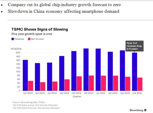
October 21, 2015 – TSMC Drops After Cutting Full-Year Capital Spending Forecast.
Taiwan Semiconductor Manufacturing Co. fell the most in almost a month after cutting its equipment budget as much as 27 percent amid slowing demand for chips and its first profit decline in three years.For a detailed account, please click here
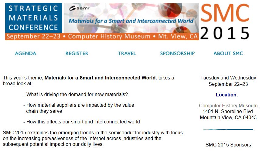
SEMI’s Strategic Materials Conference
“Materials for a Smart and Interconnected World”, Sept. 22-23, 2015, in Mountain View, CA
For More Info and TO REGISTER Click Here,
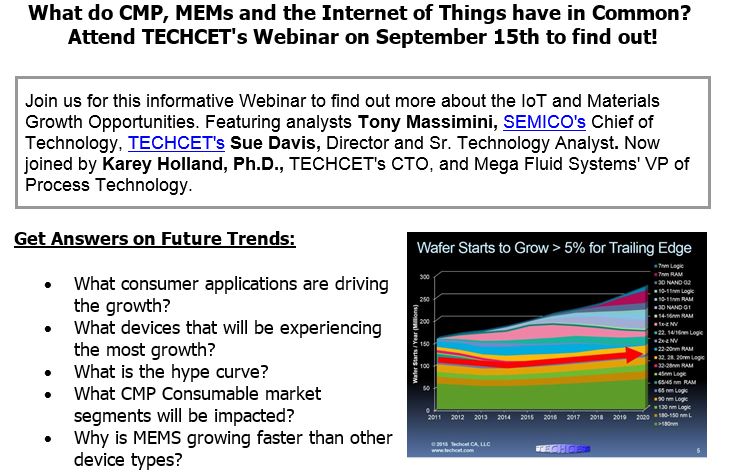
TECHCET Webinar on the IoT Market Trends and CMP Consumables – September 15, 2015, at 8:30am PST and offered again at 5:30pm PST
TO REGISTER FOR 8:30am PST Click Here, FOR 5:30pm PST Click Here
February 17, 2015 – Supply Chain Crippled by W. Coast LongShoreman Labor Dispute Over the past 9 months, the labor negotiations between the Pacific Maritime Association (an association of the major ship-owners of the West Coast) and the International Longshore and Warehouse Union, have failed to come to a full agreement, resulting in a major slowdown in shipment of products into, and out of, the US West Coast shipping ports. For a detailed account, please click here
January 29, 2015 – China Ends Its Rare Earth Ore Export Quota On December 31, 2014, China’s Ministry of Commerce (MOFCOM) and the General Administration of Customs (GAC) jointly issued two announcements, effective January 1, 2015: “Catalogue of Commodities Subject to Export License Administration in 2015 (Announcement [2014] No.94)” and “License-Issuing Catalogue in Grades of Export License Administration in 2015(Announcement [2014] No.97)”. Enterprises no longer need to provide approved export quota documents from the Ministry of Commerce for a total 8 types of goods: rare earths, tungsten and tungsten products, bauxite, coke, silicon carbide, manganese, molybdenum, and fluorspar. China’s export restrictions are strategic in the sense that they have been producing about 93% of global rare earths, up until the recent reduction to 86% due to other countries and manufacturers increasing their supply. For a detailed account, please click here
January 28, 2015 – SEMICON Korea – Presentation with Lita Shon-Roy On Wednesday, February 2, 2015, Lita Shon-Roy, president/CEO of Techcet, LLC., will be presenting on the Impact of 3D Devices on The Future of Process Materials- Trends & Opportunities. Click here for more information
November 30, 2014 – ALD/CVD High K and Metal Precursors Rising Market Forecast The market for high-κ CVD and ALD organometallic (OM) precursors continues to be on the rise, expected to grow by ~40% over the next 5 years. Leading-edge capacitors, gate dielectrics and gate electrodes as well as CVD interconnect materials (barrier materials for tungsten and copper) are of keen interest because of the high growth potential associated with the 32/28/20nm (last planar logic transistors), 22/16/14nm (first FinFET logic transistors), future logic technology nodes, as well as advanced memories. Click to Read More
November 13, 2014 – Techcet Report Advisory Service Updated and Launched This Techcet Advisory Service is an enabling component to help chip fabs, OEMs and material suppliers track, anticipate, and control the risk associated with materials supply and market competition. As appliances and home devices start anticipating our every need and access our highly capable portable devices, i.e. our iPhone 6 or our windows watch, more materials and innovative materials will be needed. Click to Read More
September 10, 2014 – Electronic Gases Report Update The 2014 market for electronic gases is anticipated to total greater than $3.2B, a few percentage points above 2013, according to Techcet Group’s report on the “Electronics Gas Market a Techcet Group Critical Materials Report.” The 2014 Electronic Gases report is one of several Critical Material Reports that Techcet generates for Sematech, but is available for purchase by non-member companies. Click to Read More
September 4, 2014 – News Flash…Strategic Materials Conference to be held in San Jose this October. The Strategic Materials Conference–SMC, is the only materials conference that attracts expert speakers and leading content relevant across the entire global materials supply chain. At SMC you’ll meet and hear renowned industry experts, along with the latest generation of technologists and logistics managers to discuss key factors supporting the growth of the microelectronics industry. Register now for the Strategic Materials Conference!
Click to Read More
August 27, 2014 – The Threat of Supply Interruption – Rare Earth Materials The concentration of production of rare earth elements (REE) in China raises the important issue of supply vulnerability for semiconductor industry, as well as for the US defense industry and many high-tech industries. They are central to numerous technologies in the computer, electronics, transportation, energy, and defense industries. Driven by an enormous number of applications, the global market for purified rare-earth starting materials is in the billion-dollar range. Click to Read More
August 27, 2014 – Silicon Wafer Market Increasing or Decreasing? Silicon wafer purchases represent the highest operating expense for many device manufacturers and as a result are a constant target for price reduction. With the continued concentration of the semiconductor manufacturing base to a few large players, silicon producers have little choice but to succumb to the price pressure. Click to Read More
May 19, 2014 – News Flash…Sputtering Targets Market Showing Strong Growth
In 2013, the semiconductor sputtering target market grew 4% to approach a total global revenue of $574 Million. Despite the emergence of alternate sources of raw materials, greater reliance on recycling, and greater competition from Chinese target suppliers, the sputtering target market is forecast to grow at a CAGR of 3.7% though 2018. While market growth will be contained to 300mm and advanced node devises, tantalum and titanium will remain the primary market drivers. JX continues to remain the market share leader of sputtering targets, as Chinese suppliers begin to make inroads by supplying to trailing-edge technologies. The primary semiconductor sputtering target suppliers are poised to supply 450mm targets as there is no insurmountable material supply or process capacity barriers. However, technical concerns including metallurgical and dimensional control for 450mm sputtering targets are currently being addressed, according to a new report from Techcet Group, “Sputtering Targets Market and Supply Chain Report 2014,” a Techcet Critical Materials Report. The outlook is for continued growth …Click here for Table of Contents