Advanced packaging and interconnect layers driving growth through ‘26
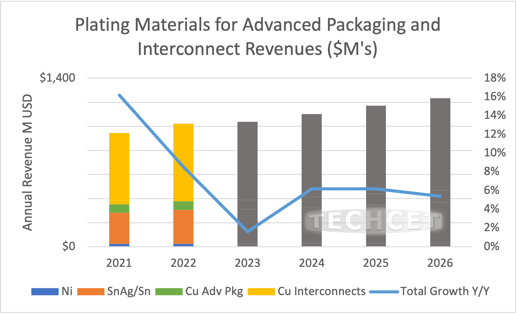
San Diego, CA, November 30, 2022: TECHCET—the advisory firm providing information on the electronics and semiconductor materials market supply-chain — announced that total deposition material revenues, including Sputtering Targets, ALD/CVD Precursors, and Metal Chemicals, will approach US$3.9 billion in 2022 and over US$4.1 billion in 2023. Growth drivers include increased use of advanced packaging with redistribution layers and copper pillar structures, and increases in interconnect layers in next generation advanced logic device nodes, soon to be followed with buried power rails and backside Cu wiring. Although TECHCET expects to see a slight slowing in the market for 2023, the overall market will see strong growth through 2026. Metal Plating alone represents >US$1.1B, expected to exceed US1.3B by 2026, as shown below.
“Longer term, demand will be driven by interest in logic, NAND and DRAM devices, and new metallization and device scheme. Multiple processing layers associated with these advanced node logic devices and 3D memory will also heighten metallization and dielectric material demand,” states Dan Tracy, Ph.D., Senior Director at TECHCET. The Total Deposition Materials market will reach US$4.7 billion or more by 2026, a 6% CAGR.
For precursors, high growth is expected for Hafnium, Cobalt, and Tungsten precursors. As the DRAM sector gears up for the transition to 3D DRAM, it will resemble the 3D NAND ramp in being a growth driver for PECVD, ALD and Etch. GAA-FETs will increase opportunities for Epitaxial Si/SiGe multi-stacks. For metal chemicals, the largest growth forecasted is from copper plating chemicals used for device level Interconnect wiring. In 2022, the copper plating market segment for advanced packaging will total US$75 million while that for copper interconnects will be approximately US$643 million. The 5-year CAGR for copper plating application is 6.1% for Advanced Packaging and 5.2% for Device Interconnects.
In the Sputtering Target segment, alternative interconnect metallization for 7nm and below, with increased use of non-Sputtering, will have potential applications using PVD metallization of Ruthenium and Molybdenum. Sputtered Molybdenum thin films can be used as a conductor metal in logic or memory interconnects and potentially for MoS2 nanosheets.
3D integration techniques have been proposed to implement a back-side power distribution Network. This network delivers power to buried power rails by Through Silicon Vias (TSV) from the wafer backside. These TSVs and backside metallization are formed by a combination of electroplating and sputtering.
For more details see, https://techcet.com/product/sputter-targets/ for sputtering targets, or for details on the ALD/CVD market segments visit https://techcet.com/product-category/ald-cvd-precursors/. For more details on the Metal Chemicals market segments and growth visit: https://techcet.com/product/metal-chemicals-for-fe-advanced-packaging/.
ABOUT TECHCET: TECHCET CA LLC is an advisory research firm focused on analyzing the electronics materials supply chains for the global semiconductor, display, solar/PV, and LED industries. TECHCET offers consulting, supply chain analysis reports, and subscription services, including the Critical Materials Council (CMC) of semiconductor fabricators and CM Data subscription services. For additional information, please contact info@cmcfabs.org, +1-480-332-8336, or go to www.techcet.com.