2023 economic slowdown to cause a short-term dip on photoresists & ancillaries
San Diego, CA, March 7, 2023: TECHCET— the electronic materials advisory firm providing business and technology information on semiconductor supply chains — is forecasting the Semiconductor Lithography materials market to dip slightly, declining -2% in 2023, which follows the downward trends of the overall semiconductor market. This slowdown is expected to be short-lived, as 2024 forecasts indicate 9.4% growth over 2023, as highlighted in TECHCET’s most recent update to the Lithography Materials Critical Materials Report™.. The Lithography materials segment, which includes photoresists and ancillaries (developers, ARCs, BARCs, EBRs, etc.), is estimated to grow 4.9% CAGR (2022-2027). The Ancillary materials segment alone is estimated to grow at a 5.1% CAGR over the same period.
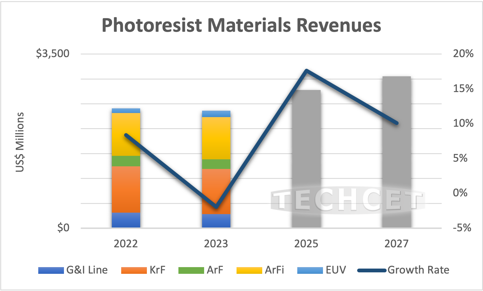
The fastest growing lithographic materials continue to be EUV and thick KrF photoresists, both of which are driven by the introduction of new technologies: advanced Logic (EUV) and memory (DUV). Metal oxide (MOX) negative tone EUV resists will also gain traction due to performance capabilities. Older technologies like G & I line are expected to also show growth in proportion to wafer starts, whereas the leading-edge materials will grow at a rate dependent on number of layers for different device types and technology nodes.
Advanced device processes will impact material usage as follows:
• Advanced logic devices will continue to require an increased number of photolithography steps per wafer start, driving for more EUV and increased 193nm (ArF) layers. However, many of the current immersion 193nm (i193nm) process steps are likely to be replaced by EUV, & i193nm related lithography materials will also decline.
• At the Gate-All-Around (GAA), also called nanosheet or nanoribbon transistors nodes, backside power rail will be added which will drive even more litho steps.
• DRAM has also started to use EUV, replacing some ArFi (i193nm) process steps. New DRAM devices are expected to increase overall litho steps per wafer.
• 3D NAND will also continue to add more layers and stacks, increasing the overall number of all process steps, including lithography steps, per wafer.
Other significant trends impacting materials include the focus on the strengthening of in-country supply-chains and chip production. This has started to impact legacy photolithography chemical makers. For example, Chinese companies are emerging as diazo photoresist makers, while Korean lithography material makers are also gaining momentum.
For more details on the Lithography Materials market and growth trajectory, including profiles on suppliers like Avantor, BASF, Brewer Science, DuPont, JSR (Inpria), Chang Chun Petrochemical, TOK, Sumitomo, FujiFilm and more, go to: https://techcet.com/product/photoresists-and-photoresist-ancillaries/.
To discuss the Lithography Materials market and semiconductor process materials issues, don’t miss the 2023 CMC Conference in Austin, Texas from April 18-20 on “Are Critical Materials for Chip Expansions Ready for Launch?” To register and for more information, visit https://cmcfabs.org/2023-cmc-conference/
ABOUT TECHCET: TECHCET CA LLC is an advisory services firm expert in market and supply-chain analysis of electronic materials for the semiconductor, display, solar/PV, and LED industries. TECHCET offers consulting, subscription service, and reports, including the Critical Materials Council (CMC) of semiconductor fabricators and Data Subscription Service (DSS). For additional information, please contact info@cmcfabs.org, +1-480-332-8336, or go to www.techcet.com.