Increasing CMP Process Steps Driving High Growth for CMP Consumables
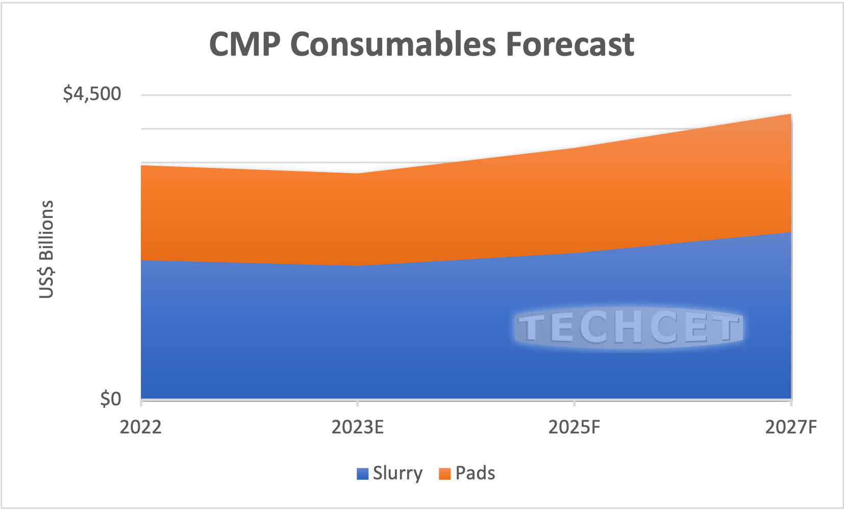
San Diego, CA, January 10, 2024: TECHCET — the advisory firm providing materials market & supply chain information for the semiconductor industry — has announced projections that the CMP Consumables market will approach US$3.5 billion in 2024, rising from the US$3.3 billion forecasted for 2023. Looking ahead to 2027, TECHCET anticipates a further surge, with the consumable materials market expected to surpass US$4.2 billion. This growth is attributed to continued global fab expansions, and the evolving demands of new device technology which require additional CMP process steps.

As highlighted in TECHCET’s Critical Materials Report™ on CMP Slurry & Pads (https://techcet.com/product/cmp-slurry-and-pads-only/), CMP continues to be one of the critical process steps to fabricate ultra-flat, low defect, and smooth surfaces, enabling advanced electronic device manufacturing to have an increased number of thin layers. Advanced technology nodes require more CMP steps – DRAM is up to 13 step, 3XXL 3DNAND requires 36 steps, and Gate-All-Around (GAA) logic requires 41 CMP steps total.
New metallization materials, such as cobalt, ruthenium, and molybdenum, are being evaluated to replace tungsten and some minimum dimension copper interconnects. These replacements will require new CMP consumables to come into play. This CMP consumable segment should experience a CAGR of over 50% as the new metallization schemes are integrated and ramped up.
Hybrid metallization, semi-damascene and hybrid-height with zero via structures are being developed to solve CMP integration challenges. Buried power rails (BPR) are helping to improve connectivity and will require 4-5 CMP steps for DRAM and 15 Cu CMP steps for GAA.
Device makers continue to look for ways to reduce consumables costs. In this current market climate, high inflation rates and the high degree of customization means that there is little chance that prices will decline for CMP consumables.
TECHCET is witnessing a high level of focus on in-line metrology, machine learning, and AI for the CMP processes. These smart manufacturing tools are being used to assist in tool-to-tool matching, contamination control, defect detection and process excursion prevention, all of which are increasing yield, improving productivity, and optimizing consumables consumption.
To purchase or view the full table of contents for TECHCET’s Critical Materials Report™ on CMP Slurry & Pads, go to: https://techcet.com/product/cmp-slurry-and-pads-only/
ABOUT TECHCET: TECHCET CA LLC is an advisory services firm expert in market and supply-chain analysis of electronic materials for the semiconductor, display, solar/PV, and LED industries. TECHCET offers consulting, subscription service, and reports, including the Critical Materials Council (CMC) of semiconductor fabricators and Data Subscription Service (DSS). For additional information, please email us here, call +1-480-332-8336, or go to www.techcet.com.
