Supply chain contraction will persist before rebounding in 2024
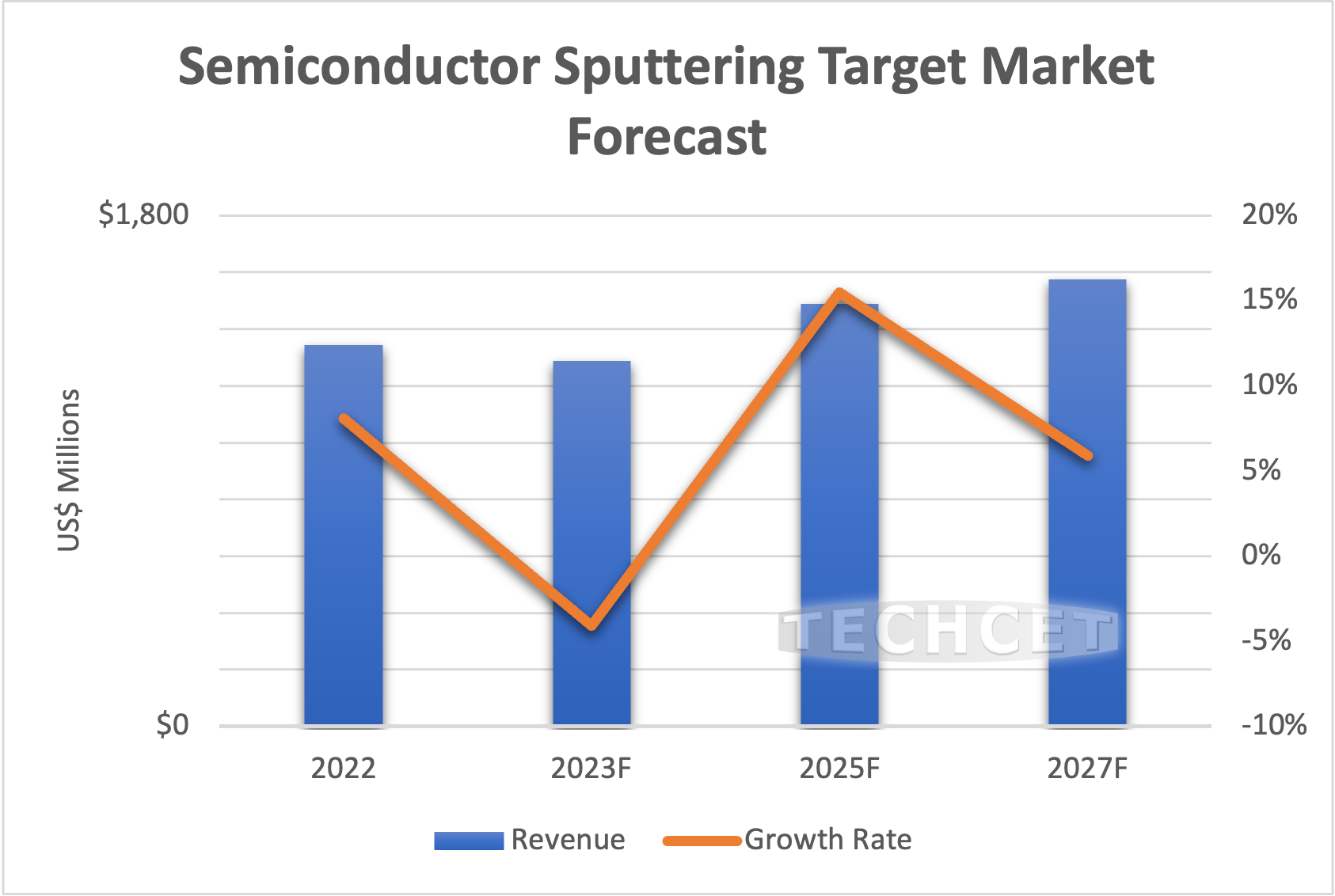
San Diego, CA, August 10, 2023: TECHCET — the electronic materials advisory firm providing business and technology information on semiconductor supply chains — states that the Semiconductor Sputtering Target market will contract to US$1.29 billion in 2023 due to the industry-wide slowdown and lower wafer starts. This decline comes after a strong year in 2022, which grew 8% over 2021 to reach US$1.34 billion. TECHCET is forecasting increased wafer starts in 2024, which will grow the targets market to US$1.39 billion, as described in TECHCET’s new Sputtering Targets Critical Materials Report™.
 .
.“The metal ore supply chain for targets is reported to be stable, though it must adapt to higher costs for metal and other process materials,” states Dan Tracy, Sr. Director at TECHCET. In addition, higher energy costs globally continue to impact the mining, smelting, and refining segments of metal supply chains. Many key metals and raw materials also have a critical reliance on sources in China, which has resulted in geopolitical concerns when it comes to supply chain management and planning for metals. With the expected ramp of new fabs in the US, target suppliers are expressing interest in alternative high-purity metal sources from within the US.
In the mid and longer term, “green energy” and “zero emission” objectives will greatly increase demand for Copper, Silver, Tungsten, Cobalt, and other metals. New mines will need to come online to meet this forecasted metal demand, with timelines being 10 years or more for mining exploration to production. Given restrictions and regulations for mining in the West, new mines will likely be located and developed in nations with less stringent mining regulations. This could thwart efforts in the semiconductor supply chain to achieve sustainability targets. Recycle, reclaim, and reuse will also be critical components of future metal supply chains to meet goals for sustainability and zero-emissions.
On the application side for targets, multiple processing layers associated with advanced node logic devices and 3D memory will accelerate PVD target demand with upper layers. Alternative interconnect metallization is expected for 7 nm and below, with increased use of non-PVD (ex. CVD/ALD) for M4 and below. Though, 3D interconnect techniques at advanced logic nodes will result in metallization requirements for back-side Power Distribution Network. This network delivers power by Through Silicon Vias (TSV) to buried power rails based on copper metallization. Growth will also rise for power devices, including SiC device technology, leading to demand for Al, Ti, and backside metallization target applications.
For more details on the Semiconductor Sputtering Target markets & supply chains, including profiles on companies such as Honeywell Electronics Materials, Grikin, JX Metals Corporation, KFMI, Linde, Materion, Tosoh SMD, and more, go to: https://techcet.com/product/sputter-targets/.
ABOUT TECHCET: TECHCET CA LLC is an advisory services firm expert in market and supply-chain analysis of electronic materials for the semiconductor, display, solar/PV, and LED industries. TECHCET offers consulting, subscription service, and reports, including the Critical Materials Council (CMC) of semiconductor fabricators and Data Subscription Service (DSS). For additional information, please contact cmcinfo@techcet.com, +1-480-332-8336, or go to www.techcet.com.